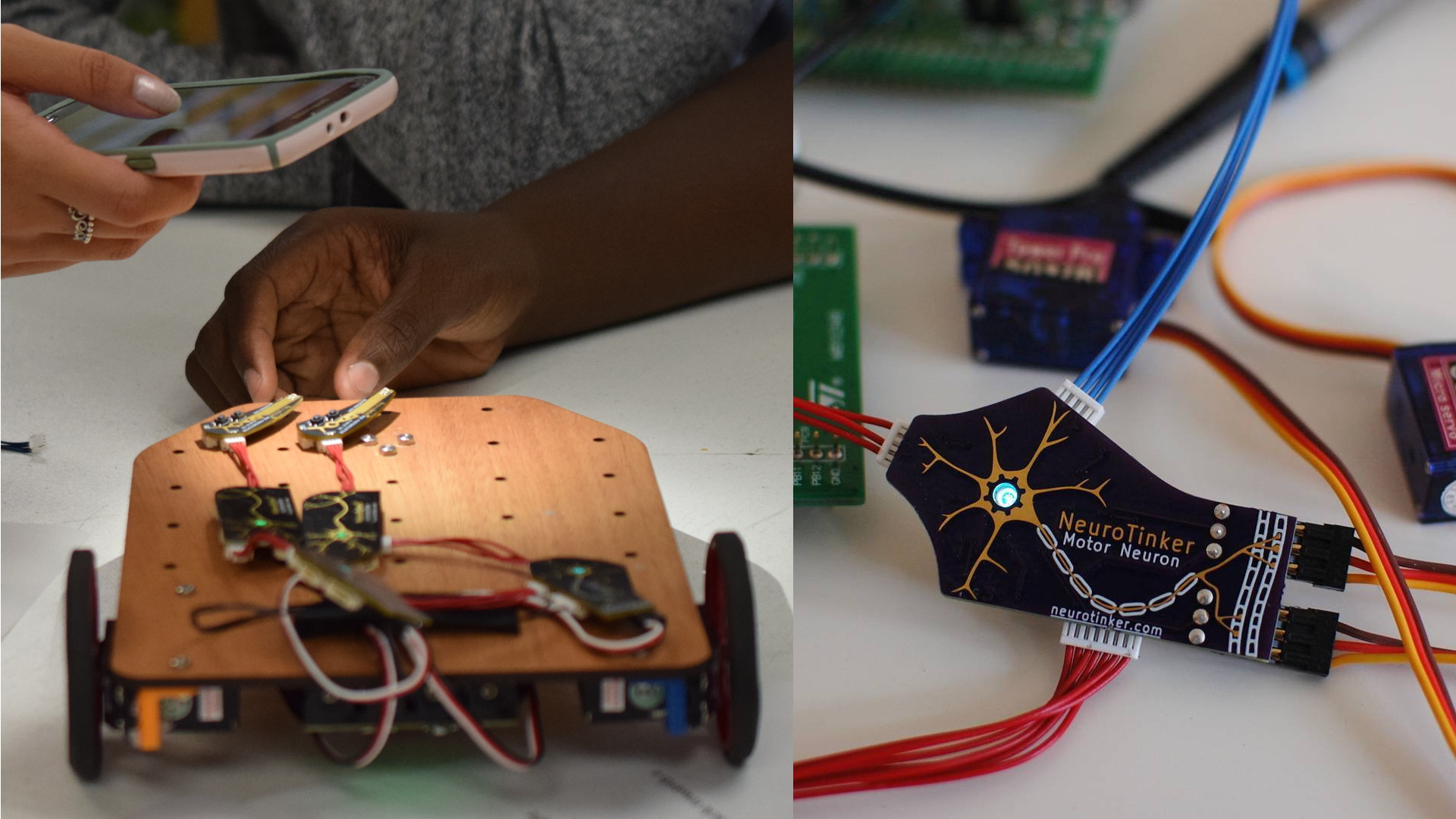
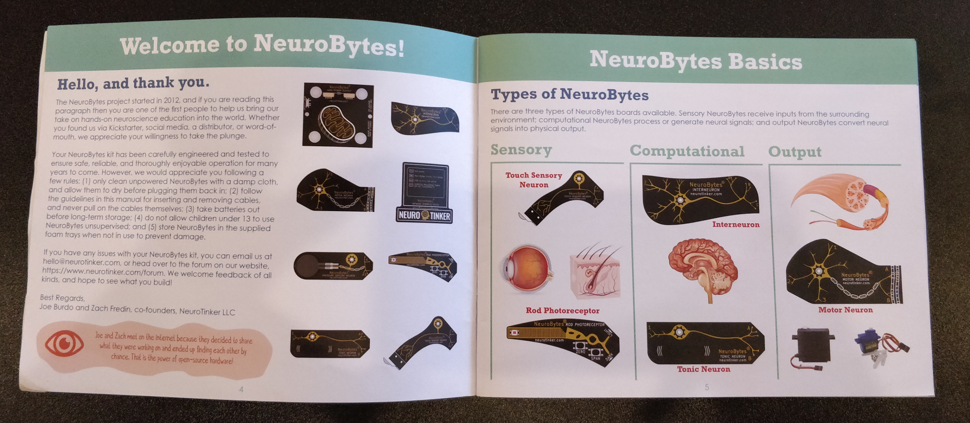
NeuroBytes
NeuroBytes® are electronic neuron simulators that help teach basic neuroscience at the high school and collegiate level. The product is open-source, modular, hands-on, and supported primarily through SBIR grants from the National Science Foundation.
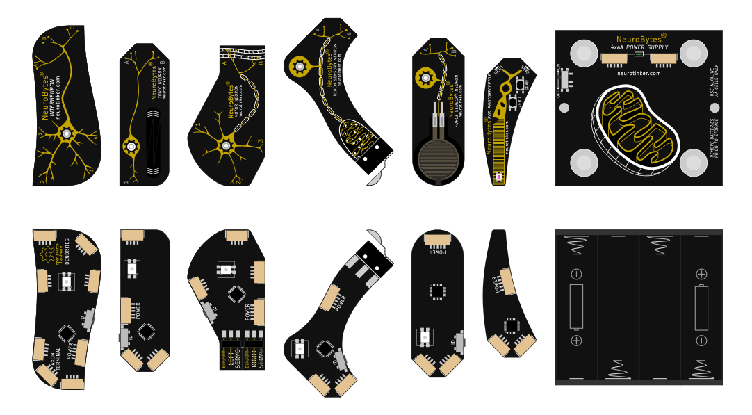
The final production NeuroBytes boards, as rendered from the original PCB design files. Left to right: Interneuron; Tonic Neuron; Motor Neuron; Touch Sensory Neuron; Rod Photoreceptor; Battery Pack. Not Shown: Network Interface Device (NID)
The NeuroBytes project led to the creation of NeuroTinker, LLC in April of 2015, and was my full time job from 2016 through mid-2019. We built roughly 1700 NeuroBytes prototypes spanning dozens of customer-driven iterations, and another 5000 boards in Dongguan, China that represent our first five hundred commercially salable kits.
Inspiration
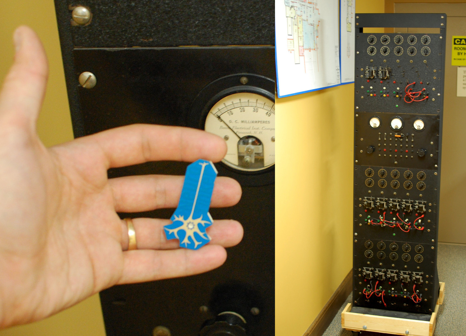
Scientists and engineers have been building electronic neuron simulators for nearly a century, ever since the electrical characteristics of the giant squid axon were discovered and Otto Schmitt built his revolutionary Nerve Computer in 1937:
Image Credit: Schmitt Trigger Nerve Computer, catalog # 85.014.001, courtesy of The Bakken Museum, Minneapolis, MN. Shown with a NeuroBytes v0.8 board.
Since then, numerous teams have built electronic neuron simulators spanning a broad range of size and sophistication. While many of these devices succeeded in their research goals, they generally failed commercially due to high unit cost.
NeuroBytes differ from earlier designs primarily because they focus on minimizing cost as a core design constraint. We recognized that while each neural element must meet some minimal level of functionality, the real power of the simulation manifests when users can build large networks; as such, each kit must contain as many devices as possible. This philosophy succeeds due to a convergence of favorable forces: the availability of low-cost high-feature microcontrollers; market acceptance of bare-PCB products such as Arduino and littleBits, allowing us to avoid expensive enclosures; and a willingness among customers to spend hundreds of dollars on sophisticated STEM education products.
Design
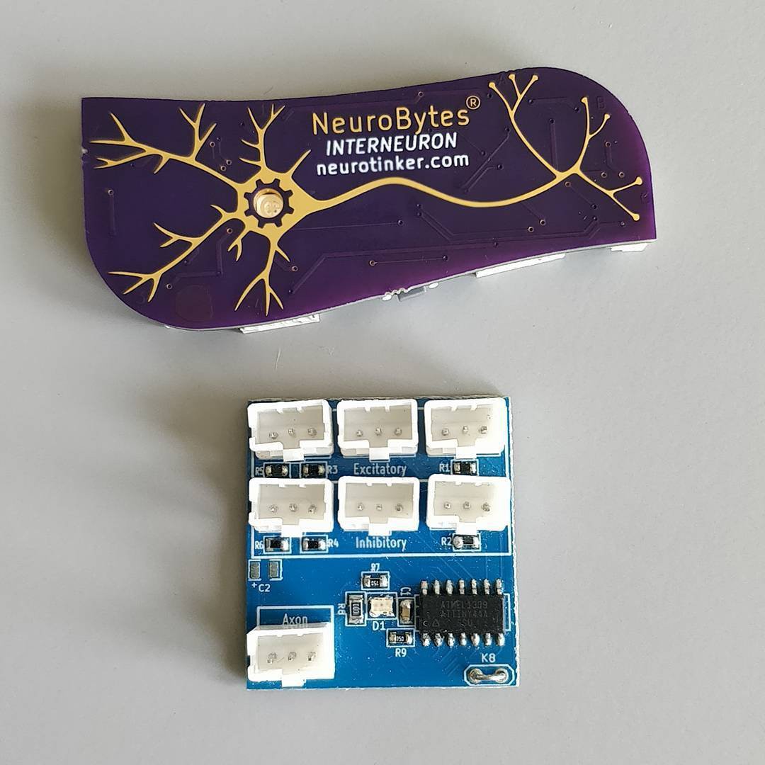
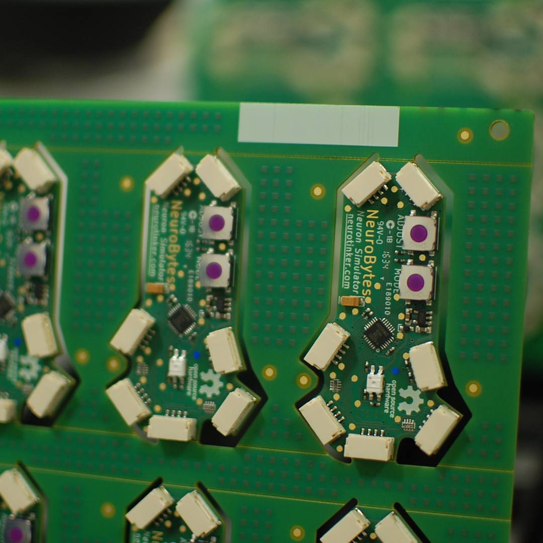
Top: Production NeuroBytes Interneuron prototype (2018); Bottom: the first pilot-scale NeuroBytes boards, v0.4 (2015)
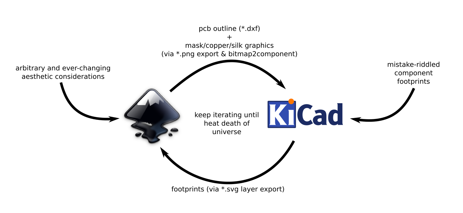
NeuroBytes have evolved to make liberal use of PCB-based graphics. These illustrations are physiologically accurate representations of actual cell structures, providing deep educational value while contributing to the unique product aesthetics. I developed these graphics using two excellent open-source tools: Inkscape, a vector graphics program, and KiCad, an EDA tool. My workflow typically follows this somewhat tongue-in-cheek diagram I made in early 2018:
Moving quickly between these tools allows me to dial in graphic design as I connect nets to form the circuit. The result is a functional electrical layout that doesn’t compromise the product’s look-and-feel:
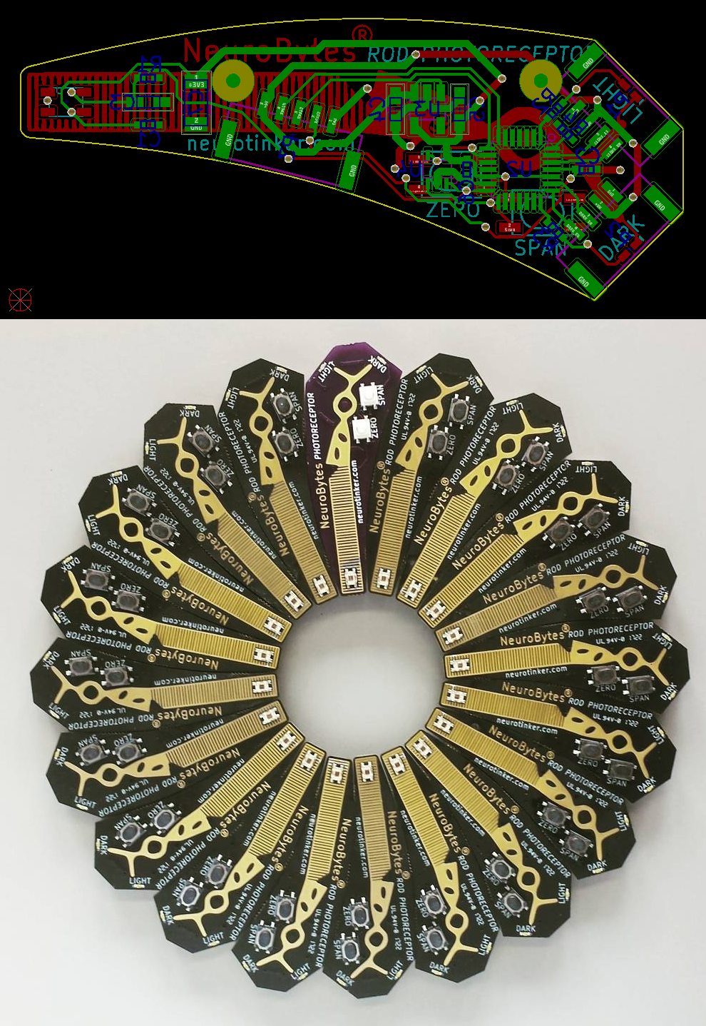
Top: Rod Photoreceptor KiCad layout showing dense, efficient routing; Bottom: Rod Photoreceptors are designed to nest, allowing the user to keep the light sensing part close together while easily breaking out wiring
Commercialization
During the course of NeuroBytes development, I scaled several generations of devices in order to test them in classrooms:
- NeuroBytes v0.4, 2015, qty ~100, hand-placed with tweezers and soldered using a modified toaster oven.
- NeuroBytes v0.8, 2016, qty 210, hand-placed with a homemade air placement tool and soldered using a stock convection oven.
- NeuroBytes v0.91, 2016, qty 500, assembled by a local contract manufacturer.
- NeuroBytes first ARM version, 2017, qty 1000 (Interneurons, Rod Photoreceptors, Motor Neurons, Touch Sensory Neurons), assembled by two different local contract manufacturers.
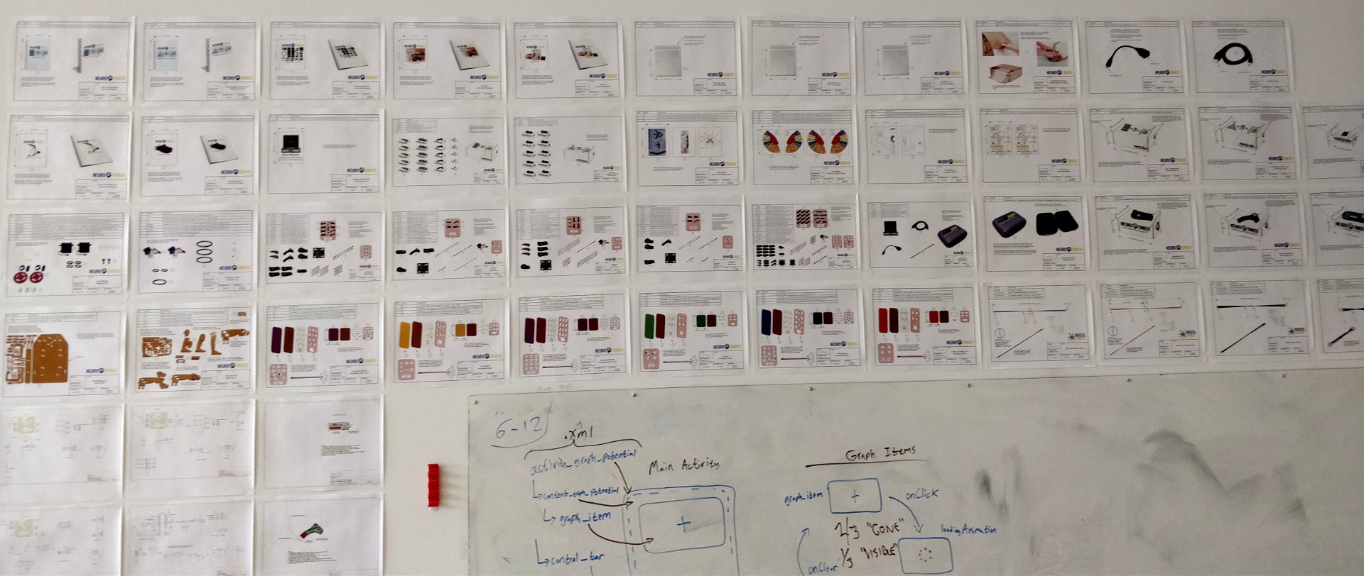
For our first major commercial run, I decided to move production to Dongguan, China, as I had been introduced to a reputable contract manufacturer and was impressed by the cost reduction: nearly 3x for printed circuit board assembly (PCBA). I also decided to engage the factory in a full turnkey effort; in addition to PCBA, they are sourcing cables, laser-cut wood parts, packaging materials, and printed documentation. Setting this up meant producing more than fifty revision-controlled engineering drawings and work instructions, all of which I printed out and gleefully taped to my office wall:
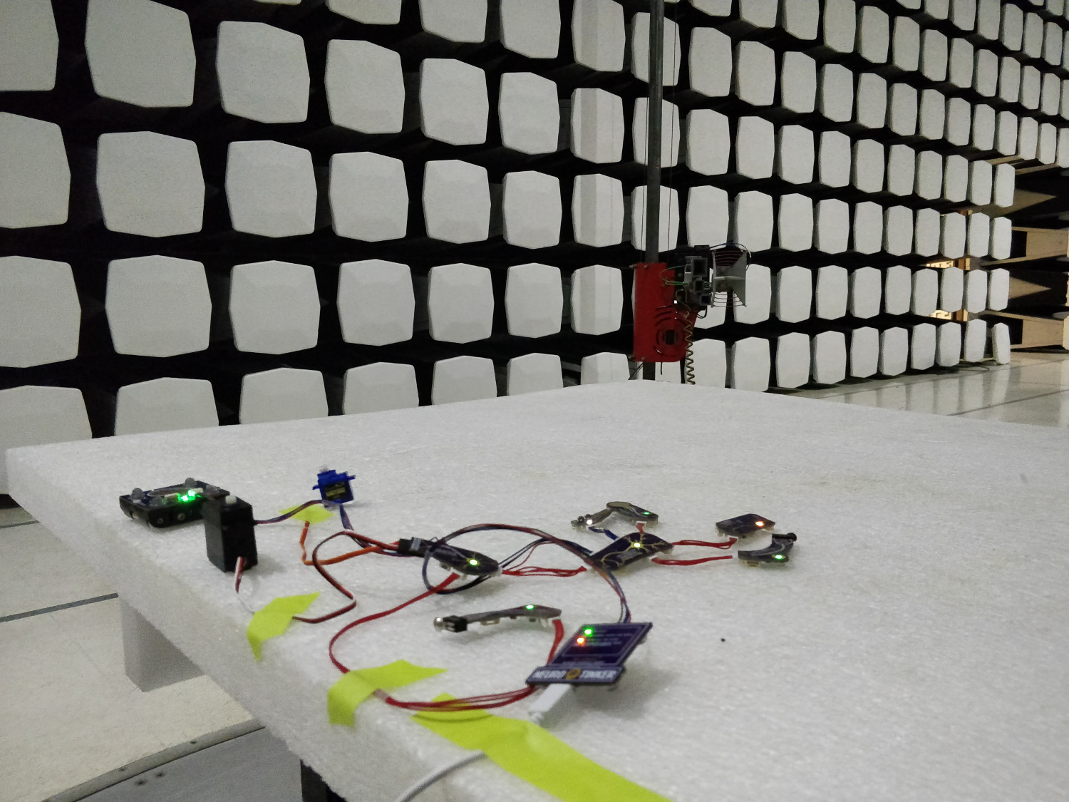
Another key part of commercialization is compliance testing. Our Kickstarter campaign resulted in sales to over a dozen countries beyond the United States, so we needed to secure CE in addition to FCC approvals.
above, a NeuroBytes circuit in the EMC anechoic testing chamber, January, 2018
While the NeuroBytes product line doesn’t have any intentional radiators, such as a Bluetooth or WiFi radio, the long cables and relatively fast data speeds resulted in enough unwanted electromagnetic radiation that we failed our first round of tests.
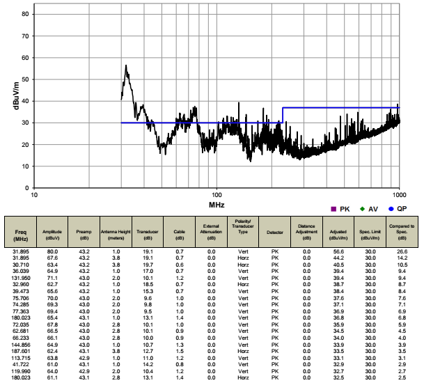
above, our first radiated emissions tests resulted in numerous peaks (black line) above the 30 dBuV/m limit (blue line)
This failure kicked off a four month redesign sprint. I bought an old but excellent spectrum analyzer which we used to trace down EMC sources through multiple PCBA revisions. We also tackled other testing challenges, including electrostatic discharge (ESD) and electromagnetic immunity (EMI), both of which are required for CE.
Documentation
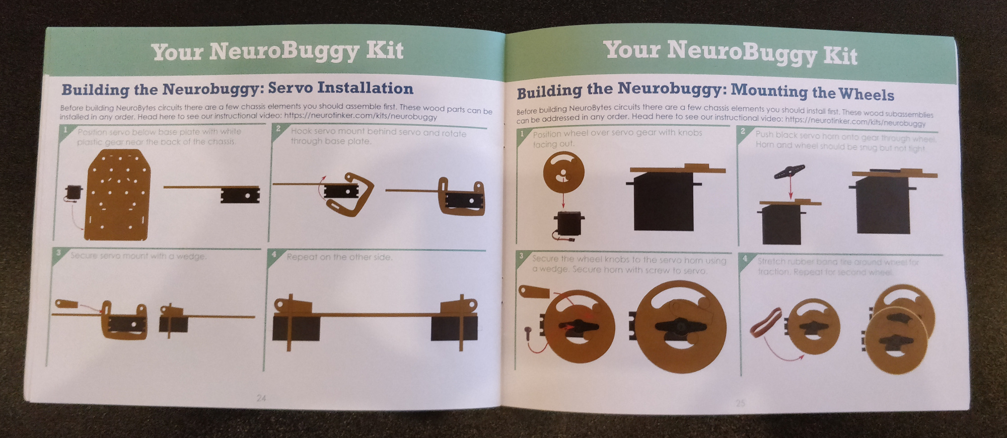
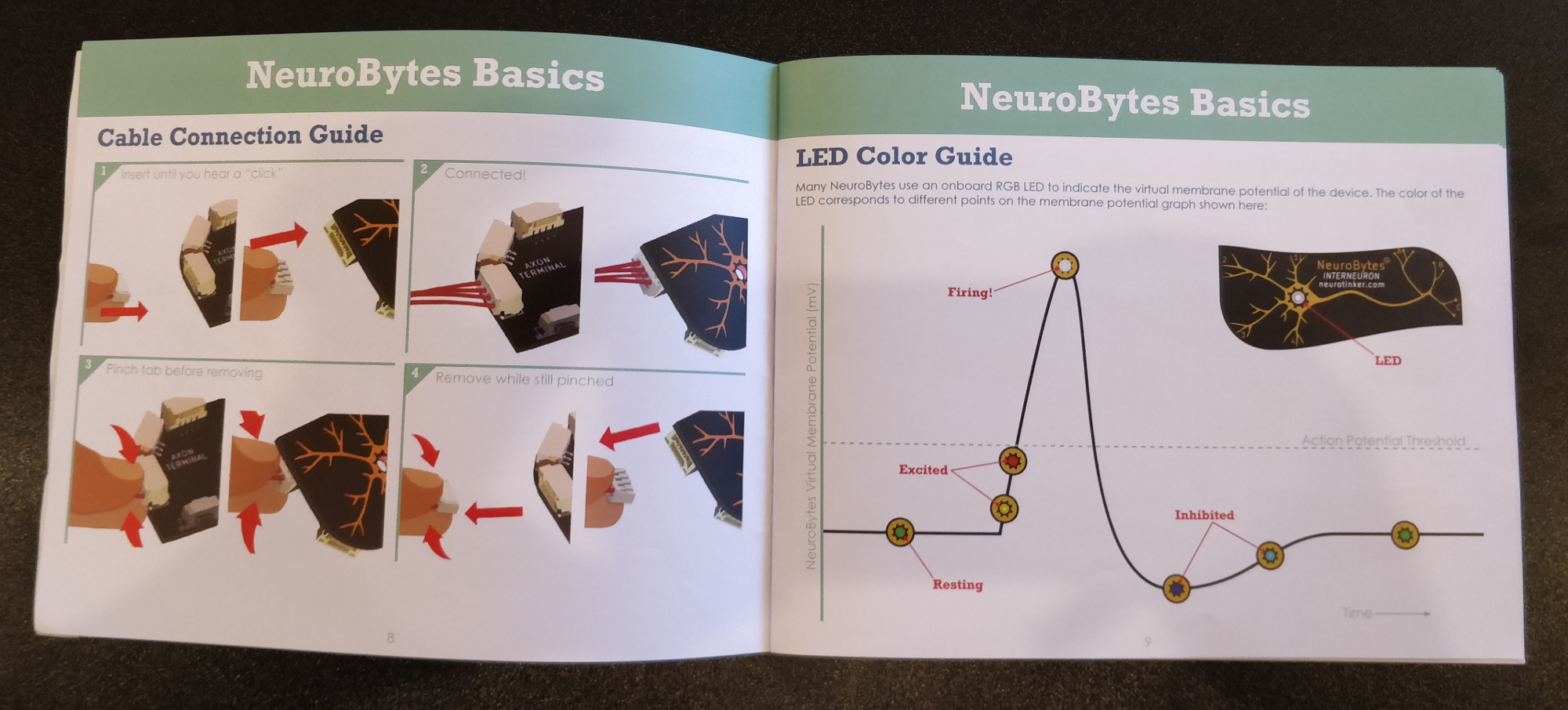
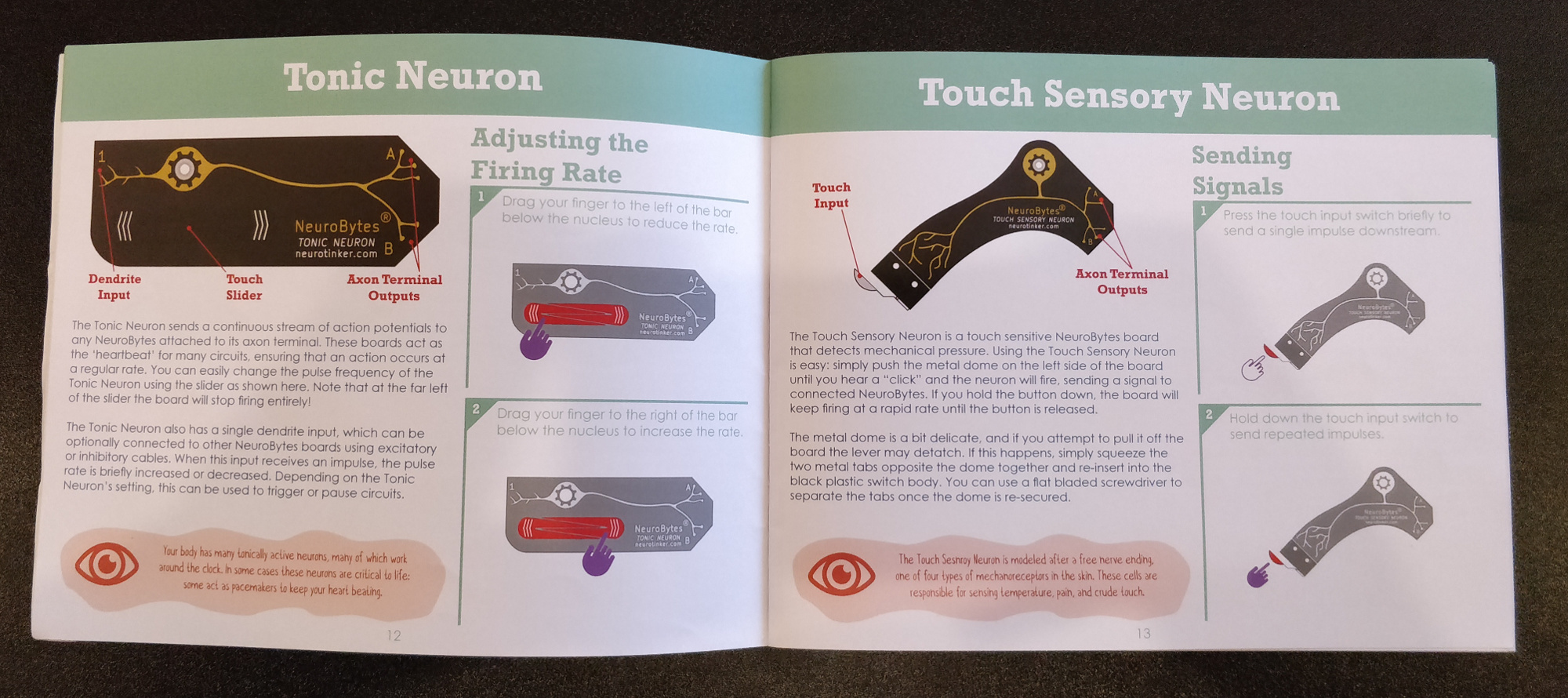
A core tenet of NeuroBytes is that they encourage hands-on experimentation rather than screen-based instruction for learning. As such, it is important that our kits include comprehensive documentation. I am particularly proud of this work, as I feel the graphic design makes our product stand out from many. Here are a few photographs of the production samples for our NeuroBuggy manual:
Resources
An exhaustive technical history of the project on hackaday.io.
Source files for the boards and physical models (CC-BY-SA 4.0).
A 2015 talk I gave at the first Hackaday Superconference on manufacturing small runs of the product.
A 2017 discussion with Chris Gammell on The Amp Hour about the project and managing SBIR grants.
Our 2017 Kickstarter video.
A 2018 talk I gave at Sketching in Hardware on the inter-neuron communications protocol we developed.
© copyright zach fredin, 2014-2019